Purpose
The RT6206BH is a synchronous step-down DC/DC converter with Advanced Constant On-Time (ACOT™) mode control. This document explains the function and use of the RT6206BH evaluation board (EVB), and provides information to enable operation, modification of the evaluation board and circuit to suit individual requirements.
Introduction
General Product Information
The RT6206BH is a synchronous step-down DC/DC converter with Advanced Constant On-Time (ACOT™) mode control. It achieves high power density to deliver up to 5.5A output current from a 4.5V to 18V input supply. The proprietary ACOT™ mode offers an optimal transient response over a wide range of loads and all kinds of ceramic capacitors, which allows the device to adopt very low ESR output capacitor for ensuring performance stabilization. In addition, RT6206BH keeps an excellent constant switching frequency under line and load variation and the integrated synchronous power switches with the ACOT™ mode operation provides high efficiency in whole output current load range. Cycle-by-cycle current limit provides an accurate protection by a valley detection of low side MOSFET and external soft-start setting eliminates input current surge during startup. Protection functions include thermal shutdown for RT6206BH.
Product Feature
-
ACOT™ Mode Enables Fast Transient Response
-
4.5V to 18V Input Voltage Range
-
5.5A Output Current
-
35mΩ Internal Low Side N-MOSFET
-
Advanced Constant On-Time Control
-
Support All Ceramic Capacitors
-
Up to 95% Efficiency
-
Discontinuous Operating Mode at Light Load
-
Adjustable Output Voltage from 0.765V to 8V
-
Adjustable Soft-Start
-
Cycle-by-Cycle Current Limit
-
Input Under-Voltage Lockout
-
Thermal Shutdown
Key Performance Summary Table
|
Key Features
|
Evaluation Board Number : PCB066_V1
|
|
Input Voltage Range
|
4.5V to 18V
|
|
Max Output Current
|
5.5A
|
|
Default Output Voltage
|
1.05V
|
|
Default Marking & Package Type
|
RT6206BHGQW, WDFN-10L 3x3
|
|
Operation Frequency
|
650kHz
|
Bench Test Setup Conditions
Headers Description and Placement
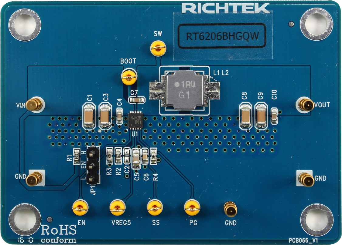
Please carefully inspect the EVB IC and external components, comparing them to the following Bill of Materials, to ensure that all components are installed and undamaged. If any components are missing or damaged during transportation, please contact the distributor or send e-mail to evb_service@richtek.com.
Test Points
The EVB is provided with the test points and pin names listed in the table below.
|
Test point/
Pin name
|
Signal
|
Comment (expected waveforms or voltage levels on test points)
|
|
VIN
|
Input voltage
|
Power input.
|
|
EN
|
Enable test point
|
Externally pulled high to enable and pulled low to disable this chip. It is internally pulled up to high when the pin is floating.
|
|
GND
|
Ground
|
The exposed pad must be soldered to a large PCB and connected to GND for maximum power dissipation.
|
|
VREG5
|
Internal Regulator Output
|
Internal Regulator Output. Connect a 1μF capacitor to GND to stabilize output voltage.
|
|
SS
|
Soft-Start Control.
|
Connect an external capacitor between this pin and GND to set the soft-start time.
|
|
PG
|
Power good test point
|
Output of power good indicator.
|
|
BOOT
|
Bootstrap supply test point
|
Bootstrap supply for high-side gate driver. Connect a capacitor between the BOOT and SW pins.
|
|
SW
|
Switch node test point
|
Connect this pin to an external L-C filter.
|
Power-up & Measurement Procedure
1. Apply a 12V nominal input power supply (4.5 < VIN < 18V) to the VIN and GND terminals.
2. Set the jumper at JP1to connect terminals 2 and 3, connecting EN to enable operation.
3. Verify the output voltage (approximately 1.05V) between VOUT and GND.
4. Connect an external load up to 5.5A to the VOUT and GND terminals and verify the output voltage and current.
Output Voltage Setting
Set the output voltage with the resistive divider (R2, R3) between VOUT and GND with the midpoint connected to FB. The output is set by the following formula :
VOUT
Schematic, Bill of Materials & Board Layout
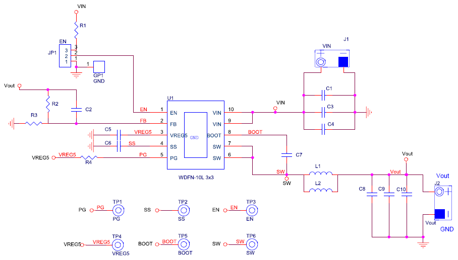
EVB Schematic Diagram
Bill of Materials
|
Reference
|
Qty
|
Part Number
|
Description
|
Package
|
Manufacture
|
|
U1
|
1
|
RT6206BHGQW
|
DC/DC Converter
|
WDFN-10L 3x3
|
RICHTEK
|
|
C1, C3
|
2
|
GRM31CR71E106KA12L
|
10µF/25V/X7R
|
C-1206
|
MURATA
|
|
C4, C10, C7
|
3
|
C1608X7R1H104KT000N
|
0.1µF/50V/X7R
|
C-0603
|
TDK
|
|
C8, C9
|
2
|
GRM31CR61A226KE19L
|
22µF/10V/X5R
|
C-1206
|
MURATA
|
|
C6
|
1
|
0603B332K500
|
3.3nF/50V/X7R
|
C-0603
|
WALSIN
|
|
C5
|
1
|
C2012X7R1E105KT
|
1µF/25V/X7R
|
C-0805
|
TDK
|
|
C2
|
1
|
|
NC
|
|
|
|
L1
|
1
|
NR8040T1R4N
|
1.4µH/7A
|
8 x 8 x 4 mm
|
TAIYO YUDEN
|
|
R2
|
1
|
|
8.25k
|
R-0603
|
|
|
R3
|
1
|
|
22.1k
|
R-0603
|
|
|
R1, R4
|
2
|
|
100k
|
R-0603
|
|
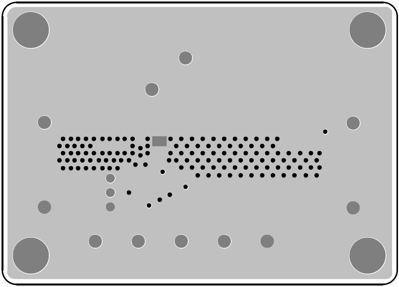
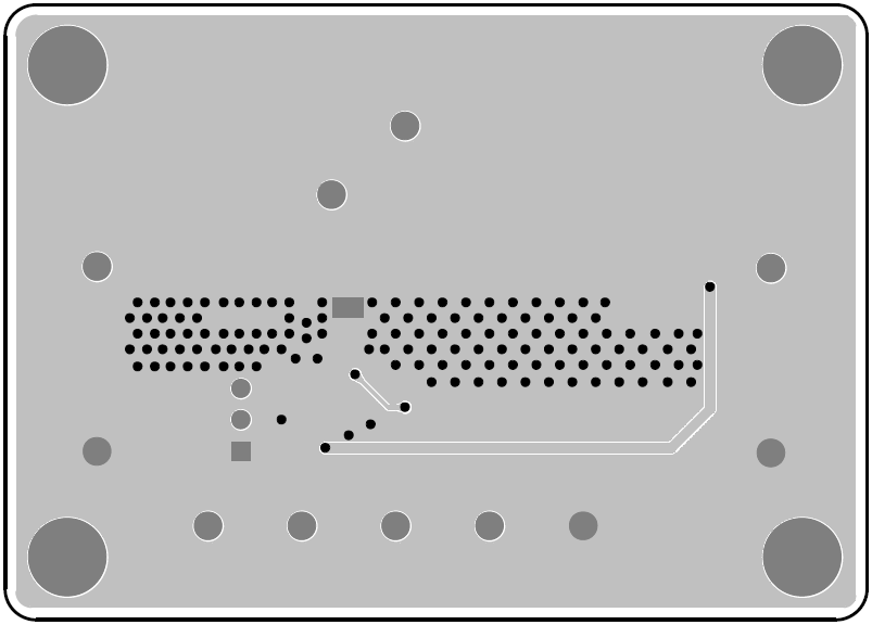
PCB Layout
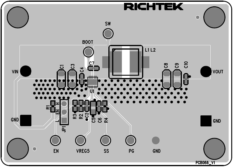
Top View (1st layer)
PCB Layout—Inner Side (2nd Layer)
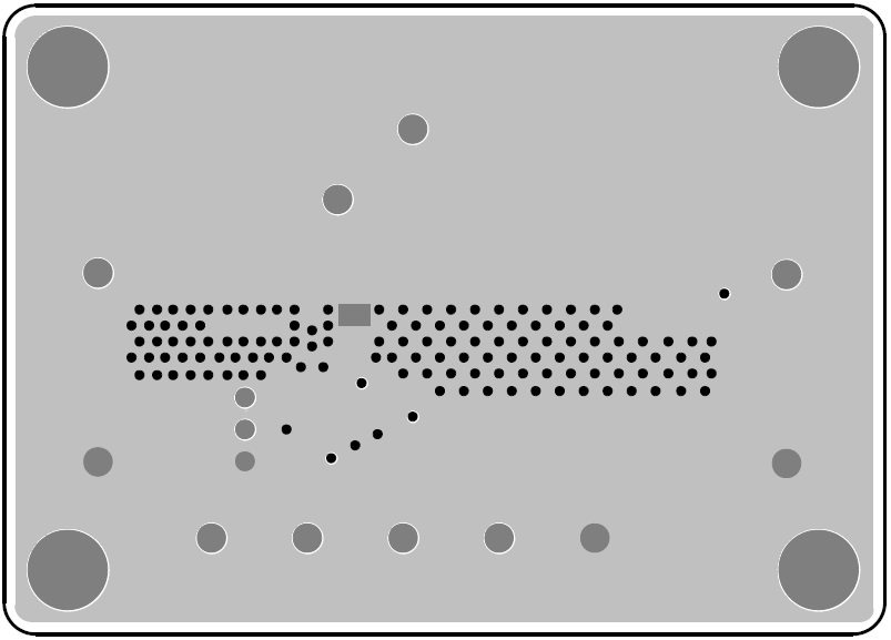
PCB Layout—Inner Side (3rd Layer)
Bottom View (4th Layer)